AVR128DA32 Feather Board
9th July 2025
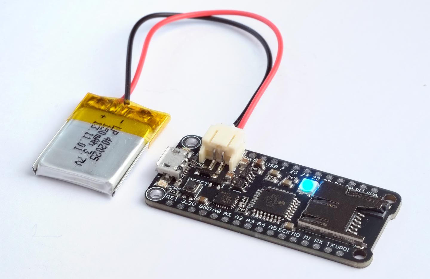
This is a Feather-format board based on the Microchip AVR128DA32. It runs at 24MHz and has 16KB of RAM and 128KB of flash:
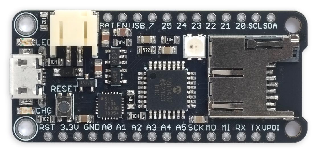
The AVR128DA32 Feather board.
It includes a MicroSD card socket, LED, and NeoPixel RGB LED. It can be powered through the USB port, or from a LiPo battery with charging through the USB port. It's an ideal board for programming in C, or in the high-level language Lisp using my uLisp interpreter.
Introduction
For some time I've been hoping that someone will make a board available based on one of my favourite microcontroller families, Microchip's AVR128DA series, in one of my favourite board form-factors, Adafruit's Feather format. Since no one has, I decided to do it myself.
The AVR128DA32 processor
What's so great about the AVR128DA series? They have the largest flash memory capacity available in the current AVR processors, 128Kbytes. More importantly, they combine this with 16Kbytes of RAM. In the AVR128DA32 this is exceptional for a 32-pin package that's relatively easy to solder: its bytes to pins ratio, measured as log(bytes)/log(pins), is 2.8, close to the maximum reached by any AVR processor; see On Bytes and Pins. The amount of RAM is important for applications such as my Lisp interpreter, uLisp.
The Feather board design
Adafruit's Feather board design is one of my favourite board form factors. It's just the right size: small enough to mount on a breadboard, but large enough to provide pins for all the important interfaces: Digital, Analogue, Serial, I2C, and SPI, together with a connector for a LiPo battery.
Adafruit have designed Feather boards for a wide range of processors, and they have also published the standard to encourage other developers to produce compatible boards: [1]. By keeping to Adafruit's specification you ensure that one of the many add-on boards, called Featherwings, will work with your board.
The main points of the Feather specification are:
- The size is 0.9" x 2.0" with 0.1" holes at each corner.
- It has one 16-pin header on the bottom side, and one 12-pin breakout strip on the top side.
- The pinouts are unified, so a Featherwing should work with all Feathers.
- It uses 3.3V logic.
- It provides a standard JST connector for a LiPo battery, with charging from the USB port, and a charge indication LED.
- It provides the following power pins: VBUS, nominally 5V from the USB port; VBAT, nominally 3.7V from the optional battery; a 3.3V output; and EN, to disable the 3.3V supply.
- It has RX and TX, SDA and SCL, and MISO, MOSI, and SCK pins in standard positions.
- There are six reserved spots for analogue pins. There are also seven spaces for general I/O pins.
- Other pins are: AREF (optional), RESET (active low), and a spare pin position.
- There must be a reset button.
I decided that I could meet this specification with the 32-pin version of the AVR128DA series.
Additional features
This AVR128DA32 Feather board also includes the following extra features beyond the basic Feather specification:
- A Micro SD card socket. This is useful when running uLisp, allowing you to load and save programs and data on an SD card.
- A Mini NeoPixel, which you can control using a uLisp assembler program.
- A spare analogue input connected to the VBAT battery voltage input via a voltage divider, so you can monitor the battery voltage from a program.
The circuit
Here's the circuit:
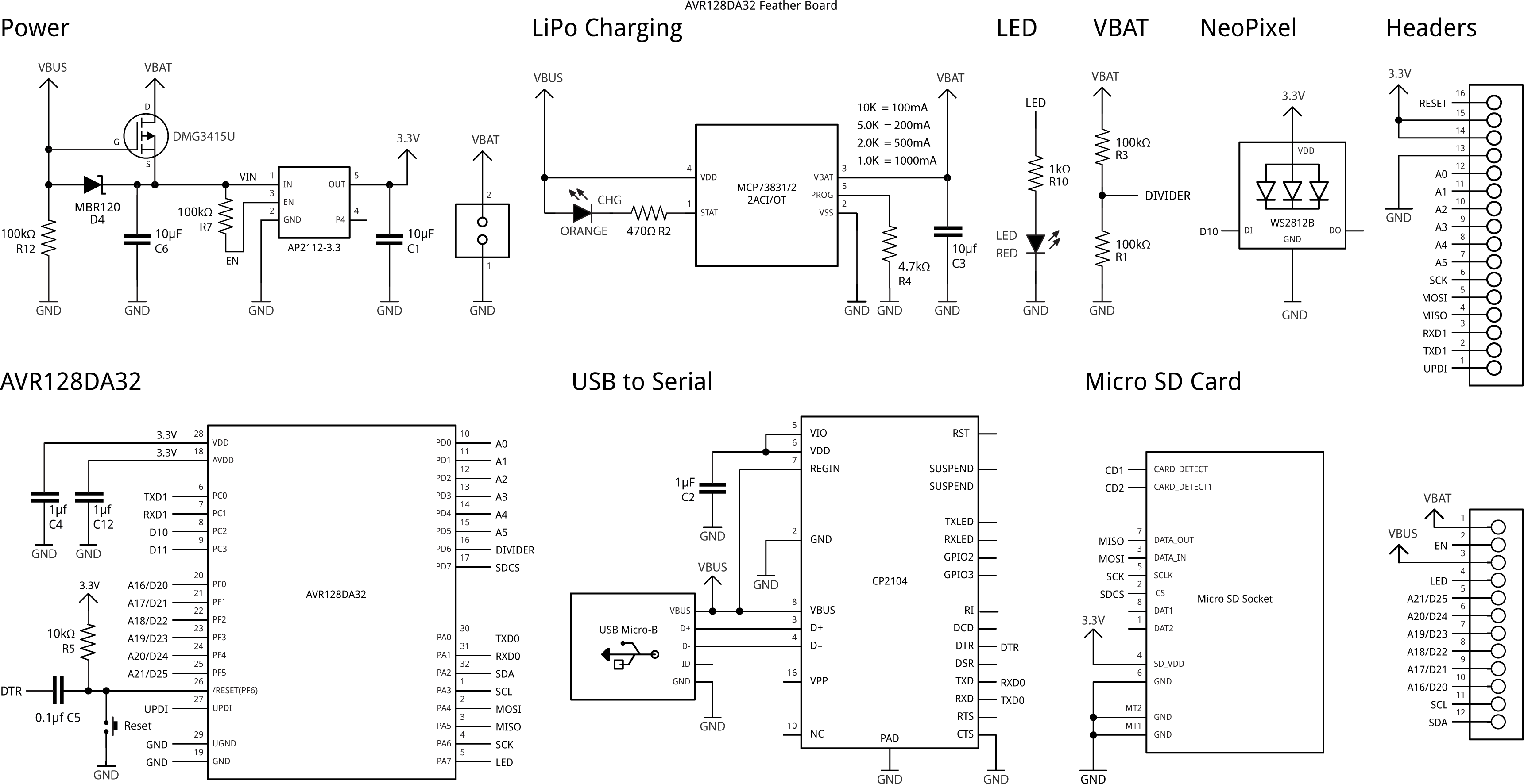
Circuit of the AVR128DA32 Feather board.
USB to Serial Converter
The board uses a Silicon Labs CP2104 USB-to-Serial converter chip to interface between the USB D+/D- signals and the AVR128DA32 RXD and TXD pins. The powering options in the datasheet for this chip are quite confusing: you can either power the chip from a 3.3V supply if you have one, by connecting it to the REGIN pin, or you can power the chip from the USB port by connecting VBUS to REGIN, in which case a 3.45V output at 100mA is available at VDD. I chose the second option; if you choose the first option the datasheet recommends connecting VBUS via a voltage divider to avoid a high VBUS pin leakage current should the 3.3V supply fail.
I tested a second prototype using the newer Silicon Labs CP2102N, which in the QFN24 package is pin compatible and functionally identical in this circuit, so you could use this if it's easier/cheaper to obtain.
Here's the parts list (click to expand):
► Parts list
Construction
I created a PCB in Eagle, and ordered a set of boards from JLCPCB.
All the components are mounted on the top of the board. There are expanded pin legends on the underside of the board:
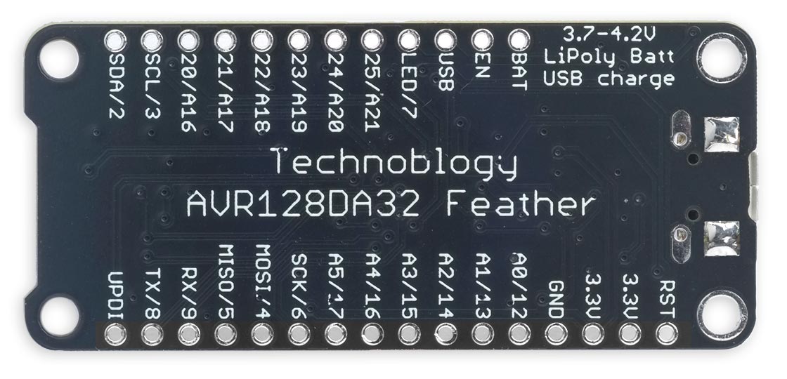
The underside of the AVR128DA32 Feather board.
All the resistors, capacitors, and LEDs are 0805 size, and the processor chip is a 32-pin TQFP package; the trickiest component to solder is the USB to Serial converter, in a QFN24 package. I used a Miniware MHP50-B5 50x50mm hotplate [2] [3] at 235°C with Chip Quik SMD291AX10T3 solder paste; the board neatly fits diagonally on the plate. I soldered the less heat-sensitive components in place first, such as the Micro SD socket, USB socket, and LiPo connector, as otherwise it's easy to knock these out of place when positioning the smaller components.
Finally, I recommend running solder through the holes in the square pads on the underside of the USB connector to firmly anchor its mounting lugs.
Testing the board
Here's the sequence I used for initially testing the board:
- Apply +5V between USB and GND while monitoring the current consumption; it should be just over 8mA. Anything much above this indicates a possible short, so disconnect quickly and check for shorts between tracks on the board.
- Apply +5V between USB and GND again, and check for +3.3V between the 3V pin and GND.
- Connect the USB connector to a 5V supply and check for +5V between the USB pin and GND, and +3.3V between the 3V pin and GND again. (It's normal for the orange CHG LED to flicker when no battery is connected.)
Next, try installing a bootloader as described in the following section.
Installing a bootloader
Although you could program the board using the UPDI pin, a better option is to install a bootloader on the AVR128DA28 chip. This will allow you to subsequently upload programs from the Arduino IDE via the serial port, and use the serial monitor for debugging.
First install Spence Konde's DxCore from GitHub: see DxCore - Installation. I used version 1.5.11.
Then, in the Arduino IDE:
- Choose the AVR DA-series (Optiboot) option under the DxCore heading on the Board menu.
- Check that the subsequent options are set as follows (ignore any other options):
Board: "AVR DA-series (Optiboot)"
Chip: "AVR128DA28"
Clock Speed: "24 MHz internal"
Bootloader Serial Port (…): "USART0 (default pins): TX PA0, RX PA1 …"
You can leave the other options at their defaults, the first option on each submenu.
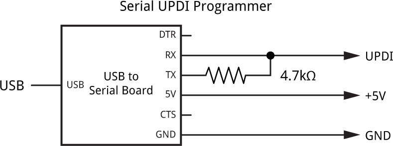
- Connect a UPDI programmer to the GND, USB (+5V), and UPDI pins on the edge connector (leave the USB connector on the AVR128DA32 board unconnected).
The recommended option is to use a USB to Serial board, such as the SparkFun FTDI Basic board [4], or a USB to Serial cable [5], connected with a 4.7kΩ resistor as follows:
- Set Programmer to the first of the "SerialUPDI - 230400 baud" options.
- Select the USB port corresponding to the USB to Serial board in the Port menu.
- Then choose Burn Bootloader from the Tools menu to upload the bootloader to the AVR128DA32.
If the upload was successful the red LED will give a series of double flashes.
Once you've installed a bootloader you can upload programs via the serial port by selecting the board from the Port option.
Using the AVR128DA28 Feather board
Pins
The function of each pin on the edge connector is described in the following table:
| Pin | Description |
| RST | Reset. |
| 3.3V | 3.3V output from the regulator for powering external circuits; up to 500mA. |
| GND | Ground. |
| A0-A5 | Analogue inputs, or general pins 12 to 17. |
| SCK, MOSI, MISO | SPI pins, or general pins 6, 4, and 5. |
| RX, TX | Serial pins, available as Serial1, or general pins 9 and 8. ‡ |
| UPDI | For programming the AVR128DA32 using UPDI. |
| SDA, SCL | I2C pins, or general pins 2 and 3. |
| 20 – 25 | General pins, or A16 to A21. |
| 7 | General pin, also connected to the red LED. |
| USB | 5V output from the USB connector. † |
| EN | Take low to disable the 3.3V regulator. |
| BAT | Direct output from the LiPo battery. |
† Can also be used to power the board from an external 5V supply, in which case the USB port should be left unconnected.
‡ These are distinct from the Serial pins 0 and 1 which are connected to the USB port.
Running a program
Here's a simple C program to test the Feather board. It's a more interesting variation of the standard Arduino Blink example. This version flashes SOS in morse code on the built-in LED:
void setup() {
  pinMode(LED_BUILTIN, OUTPUT);
}

void loop() {
  uint64_t message = 0b10000000101010001110111011100010101;
  do {
    digitalWrite(LED_BUILTIN, message & 1);
    delay(250);
    message = message >> 1;
  } while (message > 1);
}
It uses a binary constant to specify the sequence of dots and dashes. For more information about the format and timing of morse code see AM Morse-Code Transmitter.
By connecting a LiPo battery you could use the program as an emergency beacon!
Using a LiPo battery
If you have a LiPo battery connected it will power the board, but if you connect the USB cable the board will be powered by USB and the LiPo battery will be charged. The CHG LED will light when the battery is charging.
Check the polarity of your LiPo battery before connecting it; some LiPo batteries use the same connector but with the opposite polarity, which would damage the board.
The maximum recommended charge rate for a LiPo battery is 1C, which means for a 200mAh battery it should not be more than 200mA. The charge rate on the Feather board is set to 200mA by R4. If you have a larger battery and want a faster charge rate you can change this resistor; see the table on the circuit diagram.
Checking the battery voltage
Pin PD6 is connected to the battery via a potential divider, setting it at half the battery voltage, so you can check the battery voltage with analogRead(Pin_PD6).
Using uLisp
One of my objectives in designing the AVR128DA32 Feather board was to use it as a platform for my Lisp interpreter, uLisp.
Installing uLisp
Get the latest release of the AVR version of uLisp from: Download and install uLisp.
Then, in the Arduino IDE:
- Leave the option AVR DA-series (Optiboot) selected under the DxCore heading on the Board menu, and check that the subsequent options are set as before (ignore any other options):
Board: "AVR DA-series (Optiboot)"
Chip: "AVR128DA28"
Clock Speed: "24 MHz internal"
Bootloader Serial Port (…): "USART0 (default pins): TX PA0, RX PA1 …"
This time the Programmer option is irrelevant.
- Connect a USB cable to the USB connector of the AVR128DA28 Feather board.
- Select the board from the Port option. It will be a different port this time.
- Click Upload to upload uLisp to the AVR128DA28.
You should then be able to type or copy and paste Lisp programs into the field at the top of the Serial Monitor window, and click the Send button or press Return to enter them.
LED
The AVR128DA32 Feather board has a red LED connected to pin 7. You can flash "SOS" in morse code with the following program:
(defun blink ()
  (let ((message #*10101000111011101110001010100000001))
    (pinmode :led-builtin :output)
    (loop
     (dotimes (i (length message))
       (digitalwrite :led-builtin (aref message i))
       (delay 250)))))
This is similar to the C version above, except that it uses a Lisp bit array to specify the sequence of dots and dashes. Run it by typing:
(blink)
Exit from the program by entering ~ followed by return.
You can save the blink program to flash memory or SD card by typing the command:
(save-image)
You can now load it again after a reset by typing:
(load-image)
SD cards
If you want to use SD cards uncomment the line near the start of the source file before uploading uLisp:
#define sdcardsupport
You can show the contents of an SD card by typing:
(directory)
Analogue inputs
The AVR128DA32 board provides 12 analogue inputs accessible on the edge connector on pins 12 (A0) to 17 (A5) and 20 (A16) to 25 (A21). By default the resolution is 10 bits for compatibility with other Arduino boards, but you can select 12 bit resolution with:
(analogreadresolution 12)
The analogue reference voltage can be selected with analogreference. For example:
(analogreference :internal2v048)
The options are :vdd or :default, :internal1v024, :internal2v048, :internal4v096, or :internal2v5.
In addition to specifying a pin number to analogread you can also specify the keyword :adc-temperature to read the internal temperature sensor.
Pin 18 (PD6) is connected to the battery via a potential divider, setting it at half the battery voltage, so you can check the battery voltage in hundreths of a volt with:
(/ (* (analogread 18) 29) 45)
where 29/45 is a good approximation to 3.3/1024 * 2 * 100.
Analogue outputs
You can generate an 8-bit PWM analogue output on pins 2 to 8 or 12 to 17. For example, to set pin 7 to 64:
(analogwrite 7 64)
Pin 7 is also connected to the built-in LED, so that will glow at 25% brightness.
Neopixel
The AVR128DA32 board includes a mini NeoPixel, or WS2812 RGB LED, on pin 10 (PC2). The NeoPixel protocol requires pulses of 350 or 700 ns so it's not possible to control it directly from uLisp, but it's a good candidate for experimenting with machine code in uLisp.
AVR Assembler
The AVR version of uLisp includes an AVR assembler that allows you to generate machine-code functions, integrated with Lisp, and it's a good way to learn about machine code programming. The assembler itself is written in Lisp to make it easy to extend it or add new instructions. For more information see AVR assembler overview.
The following example creates a machine-code program to let you control the on-board NeoPixel LED from Lisp.
First we define constants for the PC2 port address (from the AVR128DA32 datasheet) and pin number:
(defvar port #x08)
(defvar pin 2)
Next we write an assembler macro that will generate code for the four delays the program needs by inserting a loop with a specified number of iterations, each of which takes three processor cycles:
(defun cycles3 (n)
  (list
   ($ldi 'r31 n)
   ($dec 'r31)
   ($br 'ne (- *p* 2))))
Finally here's the neopixel assembler routine:
(defcode neopixel (r g b)
  ($sbi port pin)
  ($rcall dobyte)
  ($mov 'r22 'r24)
  ($rcall dobyte)
  ($mov 'r22 'r20)
  dobyte
  ($cl 'i)
  ($ldi 'r19 #x80)
  nextbit
  ($mov 'r30 'r22)
  ($and 'r30 'r19)
  ($br 'ne one)
  zero
  ($sbi (+ 1 port) pin)
  (cycles3 2)
  ($cbi (+ 1 port) pin)
  (cycles3 2)
  ($br 'eq next)
  one
  ($sbi (+ 1 port) pin)
  (cycles3 5)
  ($cbi (+ 1 port) pin)
  (cycles3 3)
  next
  ($lsr 'r19)
  ($br 'ne nextbit)
  ($se 'i)
  ($ret))
When called from Lisp it takes three parameters, the red green and blue components of the colour. These are passed to the machine code routine in the registers r24, r22, and r20 respectively. The routine outputs the 8-bit colour values in turn, in the order g r b as required by the NeoPixel protocol, by calling the subroutine dobyte for each value. This outputs the bits in turn, MSB first, by ANDing with the mask in r19. For each bit the routine generates a zero pulse or a one pulse using the corresponding section of code.
To assemble the machine code first load the assembler from here: AVR assembler in uLisp.
Then select the above definitions and paste them into the Arduino Serial Monitor. An assembler listing will be displayed, and you can then run the routine.
For example, to set the NeoPixel to orange you can enter:
(neopixel 64 32 0)
and to turn it off enter:
(neopixel 0 0 0)
Changing colours
Finally here's a Lisp program that calls neopixel to give a sequence of slowly changing colours:
(defun glow ()
  (loop
   (dotimes (x 768)
     (neopixel (fix x) (fix (+ x 256)) (fix (+ x 512)))
     (delay 10))))

(defun fix (c)
  (setq c (mod c 768))
  (if (> c 255) (setq c (- 511 c)))
  (if (< c 0) (setq c 0))
  (/ c 4))
To run it call:
(glow)
Exit from the program by entering ~ followed by return.
Making a Lisp program run automatically on reset
You can make the AVR128DA32 board load a saved Lisp image automatically on reset, and optionally run a program, such as (glow). This is useful to make a stand-alone project that runs from a LiPo battery. To do this:
- Uncomment the option #define resetautorun at the start of the uLisp source file before uploading uLisp to the board.
- Load all the Lisp functions that you want to have available on reset.
- Save the image with save-image followed by the name of the function you want to run at reset.
For example, to run (glow) at reset give the command:
(save-image 'glow)
When you reset the board your function will load and run automatically:
Resources
Get the Eagle or Gerber files for the PCB here: https://github.com/technoblogy/avr128da32-feather.
Or order boards from OSH Park here: AVR128DA32 Feather Board.
- ^ Introducing Adafruit Feather on Adafruit.
- ^ MHP50-B5 on Adafruit.
- ^ MHP50-B5 on AliExpress.
- ^ SparkFun FTDI Basic Breakout - 5V on Sparkfun.
- ^ FTDI Serial TTL-232 USB Cable on Adafruit.
blog comments powered by Disqus