Building Gates with the AVR Event System
12th February 2024
This article shows how to use the AVR Event System to make buffers or inverters in the DA, DB, DD, EA, or EB series microcontrollers, and gives some practical examples, such as a simple Blink application:
Using the Event System on an AVR128DA28 to blink an LED without running a program.
Introduction
If you're designing a project based on an AVR processor and you find you need a few buffers or inverters, one option would be to add a CMOS gate package to your circuit. However, as I found in a recent project, you can often solve the application without any extra components by using the AVR Event System.
The Event System is an under-appreciated aspect of the AVR microcontrollers, probably because it's a bit unintuitive to use. Although this article only covers simple applications, using buffers or inverters, it should be helpful in understanding how to use the Event System to interconnect other peripherals in the processor.
History
Microchip introduced the Event System as a feature of their new ATtiny 1-series processors, and it has been included in all AVR processors released since then. There have been three iterations of the Event System:
- The original version, introduced with the ATtiny 0-series and 1-series, distinguishes between asynchronous channels and synchronous channels.
- A second version, introduced with the AVR DA, DB, and DD series processors, simplified the use of channels in events by having just one type of channel; events are synchronous or asynchronous depending on which peripheral is being used. This version of the Event System is also used in the ATtiny 2-series.
- A third version, introduced with the AVR EA and EB series processors, extends the second version with more flexibility about which channels you can use with each peripheral.
This tutorial only deals with the second and third versions of the Event System.
How it works
The Event System effectively allows you to configure patch leads inside the microcontroller, going between specified peripheral outputs and peripheral inputs. This article is going to look at the simplest application of this, connecting an I/O input pin to an I/O output pin to make a buffer or inverter.
Terminology
The Event System avoids using the terms "input" or "output" because this could get confusing. For example, the input to the Event System could be the output from a Timer/Counter. It therefore uses the terms "event generator" for the signal initiating the event, and "event user" for the signal that will be changed by the event.
Event generator
In our application the signal coming from the I/O port input is the event generator. You can usually use any I/O port input as an event generator.
There can only be one event generator; it wouldn't make sense to have more than one input, because there would be a conflict if two inputs had different logic levels.
Event user
In our application the I/O port output that will be changed by the event is the event user. You can have multiple event users for an event.
There is one event user available per port, and the signal is called EVOUTA to EVOUTG. The following table shows which pins the Event System allows you to use as the event user for different members of the Dx and Ex series microcontrollers, and how many gates you could therefore create:
| Series | Pincount | EVOUTA | EVOUTB | EVOUTC | EVOUTD | EVOUTE | EVOUTF | EVOUTG | Gates |
| DA | 28 | PA2, PA7 | PC2 | PD2, PD7 | 3 | ||||
| 32 | PA2, PA7 | PC2 | PD2, PD7 | PF2 | 4 | ||||
| 48 | PA2, PA7 | PB2 | PC2, PC7 | PD2, PD7 | PE2 | PF2 | 6 | ||
| 64 | PA2, PA7 | PB2, PB7† | PC2, PC7 | PD2, PD7 | PE2, PE7† | PF2 | PG2, PG7 | 7 | |
| DB | 28 | PA2, PA7 | PC2* | PD2, PD7 | 3 | ||||
| 32 | PA2, PA7 | PC2* | PD2, PD7 | PF2 | 4 | ||||
| 48 | PA2, PA7 | PB2 | PC2*, PC7* | PD2, PD7 | PE2 | PF2 | 6 | ||
| 64 | PA2, PA7 | PB2, PB7 | PC2*, PC7* | PD2, PD7 | PE2, PE7 | PF2 | PG2, PG7 | 7 | |
| DD | 14 | PC2* | PD7 | PF7 | 3 | ||||
| 20 | PA2, PA7 | PC2* | PD7 | PF7 | 4 | ||||
| 28 | PA2, PA7 | PC2* | PD2, PD7 | PF7 | 4 | ||||
| 32 | PA2, PA7 | PC2* | PD2, PD7 | PF2, PF7 | 4 | ||||
| EA | 28 | PA2, PA7 | PC2 | PD2, PD7 | PF7 | 4 | |||
| 32 | PA2, PA7 | PC2 | PD2, PD7 | PF2, PF7 | 4 | ||||
| 48 | PA2, PA7 | PB2 | PC2, PC7 | PD2, PD7 | PE2 | PF2, PF7 | 6 | ||
| EB | 14 | PA2, PA7 | PC2 | PD7 | PF7 | 4 | |||
| 20 | PA2, PA7 | PC2 | PD7 | PF7 | 4 | ||||
| 28 | PA2, PA7 | PC2 | PD2, PD7 | PF7 | 4 | ||||
| 32 | PA2, PA7 | PC2 | PD2, PD7 | PF2, PF7 | 4 |
Pincount: The size of the package.
EVOUTA – EVOUTG: The pins available for the event user EVOUT signals.
Gates: The maximum number of buffers or inverters you can make.
* These pins support Multi-Voltage I/O (MVIO) (see Multi-Voltage Input/Output).
† According to the AVR128DA errata: port pins PB[7:6] and PE[7:4] are not connected to the event system [1].
Where two pins are shown for a port, such as PA2 and PA7, these are alternatives and you can't use both. Where available, you select the alternative output on bit 7 using the PORTMUX EVSYSROUTEA register.
Channels
Each patch lead, linking an event generator with one or more event users, is called a "channel". Depending on the processor there can be between 6 and 10 channels, numbered from CHANNEL1 to CHANNEL10.
The way in which channels and event generators interact is different between the DX series and EX series processors, as described in the following sections.
Channels and event generators in the Dx series
In the DA, DB, and DD series there are constraints on which channels you can use with event generators in each port, as shown in the following table:
| Ports | Channels |
| PORTA and PORTB | CHANNEL0 and CHANNEL1 |
| PORTC and PORTD | CHANNEL2 and CHANNEL3 |
| PORTE and PORTF | CHANNEL4 and CHANNEL5 |
| PORTG | CHANNEL6 and CHANNEL7 |
So you can use at most two I/O pins from PORTA and PORTB, two from PORTC and PORTD, and so on.
If you try to use an I/O pin with a channel that doesn't support it you'll get a compile error, such as:
'EVSYS_CHANNEL2_PORTA_PIN0_gc' was not declared in this scope
Channels and event generators in the Ex series
The EA and EB series are slightly more flexible: you can use any two I/O pins from each port, and you can associate them with any of the available channels. This means that the commands to configure them are slightly different.
The two event generator pins in each port are called EVGEN0 (or EV0) and EVGEN1 (or EV1), and a new EVGENCTRLA register for each port lets you specify which two pins correspond to EVGEN0 and EVGEN1; see the example Blink on EA series below.
It's asynchronous
Channels between I/O pins are asynchronous; in other words, their switching is independent of the processor's clock rate and could run at a higher frequency than the clock rate.
Multi-Voltage Input/Output
The DB and DD series support Multi-Voltage Input/Output (MVIO), which allows you to power the I/O pins on PORTC from a different voltage rail, VDDIO2. This lets you make a buffer or inverter that performs logic-level translation: for example, it would let you make a buffer that translates the logic level of another pin on the processor that is not available on PORTC.
Tutorial
To create a gate using the Event System on the Dx series microcontrollers you need to go through the following steps:
- Choose the I/O pin you want to use as the event generator; this will be the input of the gate.
- Choose the channel you want to use to link the event generator to the event user; depending on the port you used in the previous step there may be two options; see Channels and event generators above.
- Link the event generator to the channel.
For example, if you chose PA1 as the event generator and CHANNEL0 as the channel, give the command:
EVSYS.CHANNEL0 = EVSYS_CHANNEL0_PORTA_PIN1_gc;
- Choose the I/O pin you want to use as the event user, from the output pins table above. This will be the output of the gate.
- Link the same channel to the event user.
For example, if you chose PA2 as the event user, this is the default option for EVOUTA and you would give the command:
EVSYS.USEREVSYSEVOUTA = EVSYS_USER_CHANNEL0_gc;
Alternatively, if you chose PA7 as the event user, this is the alternate option for EVOUTA and you would need to give the commands:
PORTMUX.EVSYSROUTEA = PORTMUX_EVOUTA_ALT1_gc;
EVSYS.USEREVSYSEVOUTA = EVSYS_USER_CHANNEL0_gc;
Note that you don't need to configure the EVOUT pin as an output; this is done automatically.
- Finally, if you want to make an inverter rather than a buffer, invert the input or the output.
For example, with the above options you could invert PA1 with:
PORTA.PIN1CTRL = PORT_INVEN_bm;
Applications
For the following applications I've used an AVR128DA28 in a PDPIP package because it is convenient to use on a breadboard, but you could use almost any DA, DB, or DD series processor; the memory requirements are minimal. For the EA example I've used a Curiosity Nano board.
Blink
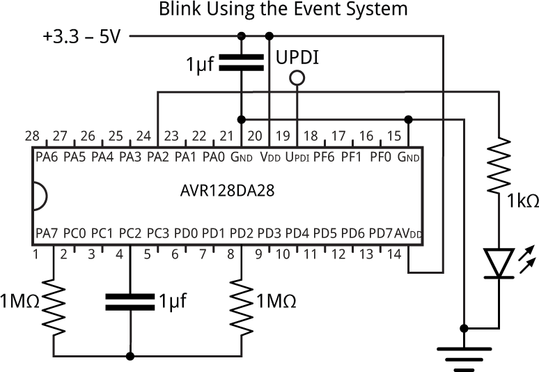
The first application is a simple RC oscillator, using two inverters and a buffer, to flash an LED at about 1Hz like the classic Arduino Blink program. The difference is that this blinking LED works without running a program.
Here's the equivalent circuit:
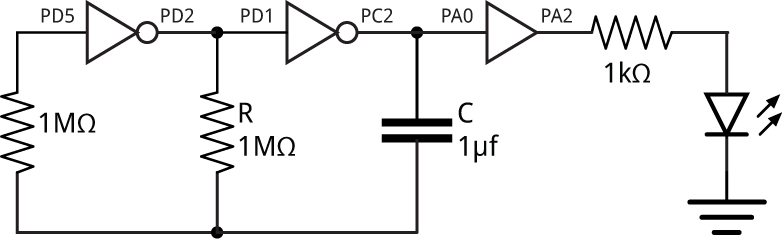
The third gate, which can be a buffer or an inverter, drives the LED to isolate it from affecting the timing of the RC oscillator. The frequency is given by:
Here's the full circuit showing the wiring of the AVR128DA28:
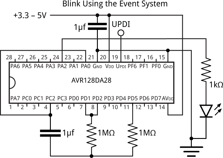
And here are the statements for the AVR128DA28 to configure the three gates:
void setup() {
  // Inverter: Channel 2, PD5 input, PD2 output
  EVSYS.CHANNEL2 = EVSYS_CHANNEL2_PORTD_PIN5_gc;      // PD5 generator on CHANNEL2
  EVSYS.USEREVSYSEVOUTD = EVSYS_USER_CHANNEL2_gc;     // EVOUTD (PD2) CHANNEL2 user
  PORTD.PIN2CTRL = PORT_INVEN_bm;                     // Invert output PD2

  // Inverter: Channel 3, PD1 input, PC2 output
  EVSYS.CHANNEL3 = EVSYS_CHANNEL3_PORTD_PIN1_gc;      // PD1 generator on CHANNEL3
  EVSYS.USEREVSYSEVOUTC = EVSYS_USER_CHANNEL3_gc;     // EVOUTC (PC2) CHANNEL3 user
  PORTC.PIN2CTRL = PORT_INVEN_bm;                     // Invert output PC2

  // Buffer: Channel 0, PA0 input, PA2 output
  EVSYS.CHANNEL0 = EVSYS_CHANNEL0_PORTA_PIN0_gc;      // PA0 generator on CHANNEL0
  EVSYS.USEREVSYSEVOUTA = EVSYS_USER_CHANNEL0_gc;     // EVOUTA (PA2) CHANNEL0 user
}

void loop() { }
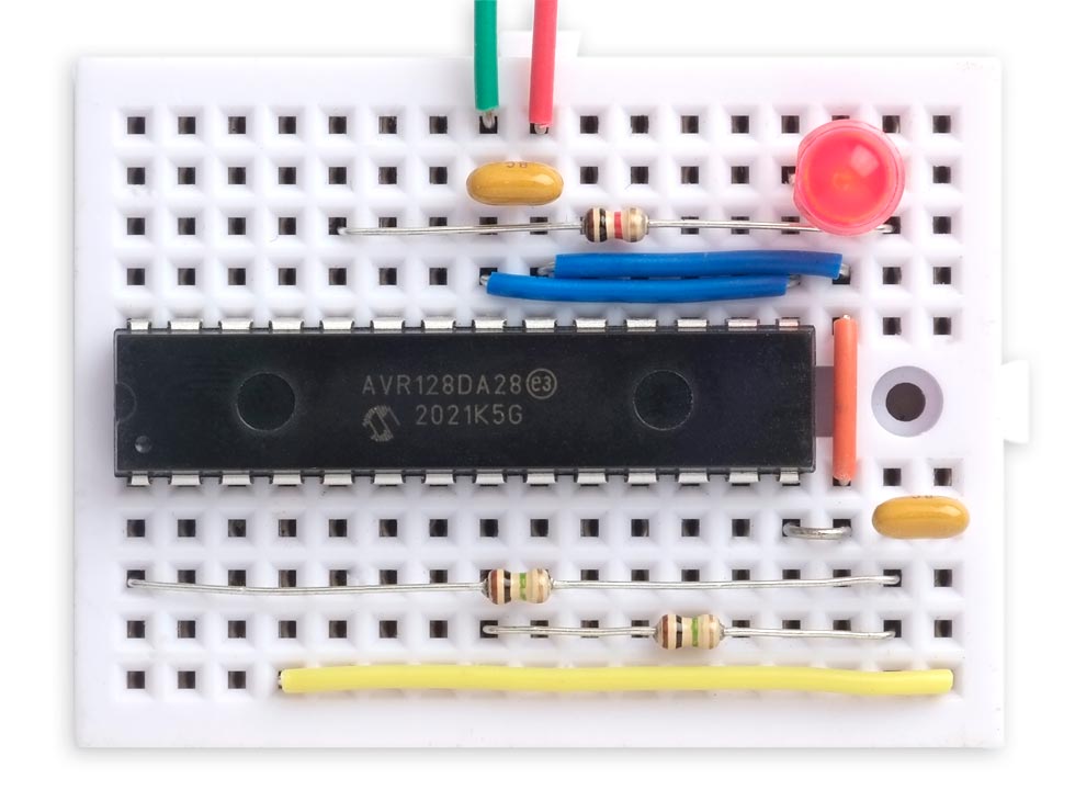
I tested it on a mini breadboard:
The Blink application using the Event System on an AVR128DA28.
It should work with any member of the AVR DA, DB, or DD family.
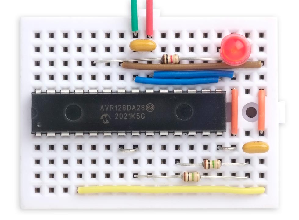
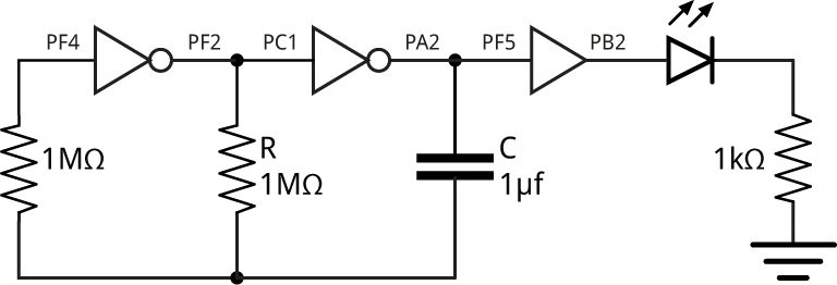
Blink using fewer pins
The previous version of Blink uses six external I/O pins, two for each gate. However, we can save two I/O pins by using the event system to make the connections between PD2 and PD1, and between PC2 and PA0. We just need to specify the same output pin from each gate as the input pin for the next gate in the cascade.

To make this work I've had to use PA7 instead of PD5 as the event generator for the first inverter, because we can't have three generators from PORTC and PORTD; see Channels and Event Generators above.
Here's the modified circuit:
Here are the statements to configure this:
void setup() {
  // Inverter: Channel 0, PA7 input, PD2 output
  EVSYS.CHANNEL0 = EVSYS_CHANNEL0_PORTA_PIN7_gc;      // PA7 generator on CHANNEL0
  EVSYS.USEREVSYSEVOUTD = EVSYS_USER_CHANNEL0_gc;     // EVOUTD (PD2) CHANNEL0 user
  PORTD.PIN2CTRL = PORT_INVEN_bm;                     // Invert input and output PD2

  // Inverter: Channel 3, PD2 input, PC2 output
  EVSYS.CHANNEL3 = EVSYS_CHANNEL3_PORTD_PIN2_gc;      // PD2 generator on CHANNEL3
  EVSYS.USEREVSYSEVOUTC = EVSYS_USER_CHANNEL3_gc;     // EVOUTC (PC2) CHANNEL3 user

  // Buffer: Channel 2, PC2 input, PA2 output
  EVSYS.CHANNEL2 = EVSYS_CHANNEL2_PORTC_PIN2_gc;      // PC2 generator on CHANNEL2
  EVSYS.USEREVSYSEVOUTA = EVSYS_USER_CHANNEL2_gc;     // EVOUTA (PA2) CHANNEL2 user
}

void loop() { }
There's one other subtlety: the PORT_INVEN configuration inverts both the input and output of an I/O pin. Therefore the statement:
PORTD.PIN2CTRL = PORT_INVEN_bm;
inverts both the output of the first gate and the input of the second gate. Thus, we no longer need the statement:
PORTC.PIN2CTRL = PORT_INVEN_bm;
otherwise the middle gate will be inverted twice.
Here's the circuit on a breadboard:
A simpler version of the Blink application, using the Event System on an AVR128DA28.
Blink on EA series
I also tested the same Blink application on an AVR64EA48, using the Microchip Curiosity Nano board. To make it easier to lay the components out on the breadboard I changed the I/O pins used for the gates, but it's essentially the same circuit as the earlier examples:
Here are the statements to implement this circuit:
void setup() {
  // Inverter: Channel 0, PF4 input, PF2 output
  PORTF.EVGENCTRL = PORT_EVGEN0SEL_PIN4_gc;           // PF4 generator for PORTF EV0
  EVSYS.CHANNEL0 = EVSYS_CHANNEL_PORTF_EV0_gc;        // PORTF EV0 goes to CHANNEL0
  EVSYS.USEREVSYSEVOUTF = EVSYS_USER_CHANNEL0_gc;     // EVOUTF (PF2) CHANNEL0 user
  PORTF.PIN2CTRL = PORT_INVEN_bm;                     // Invert output PF2

  // Inverter: Channel 1, PC1 input, PA2 output
  PORTC.EVGENCTRL = PORT_EVGEN0SEL_PIN1_gc;           // PC1 generator for PORTC EV0
  EVSYS.CHANNEL1 = EVSYS_CHANNEL_PORTC_EV0_gc;        // PORTC EV0 goes to CHANNEL1
  EVSYS.USEREVSYSEVOUTA = EVSYS_USER_CHANNEL1_gc;     // EVOUTA (PA2) CHANNEL1 user
  PORTA.PIN2CTRL = PORT_INVEN_bm;                     // Invert output PA2

  // Buffer: Channel 2, PF5 input, PB2 output
  PORTF.EVGENCTRL |= PORT_EVGEN1SEL_PIN5_gc;          // PF5 generator for PORTF EV1
  EVSYS.CHANNEL2 = EVSYS_CHANNEL_PORTF_EV1_gc;        // PORTF EV1 goes to CHANNEL2
  EVSYS.USEREVSYSEVOUTB = EVSYS_USER_CHANNEL2_gc;     // EVOUTB (PB2) CHANNEL2 user
}

void loop() { }
On the EA series there's an additional step in configuring each gate: you have to choose whether to send the event generator on each port to EV0 or EV1, and configure the EVENCTRL register for that port accordingly. Note that we have two event generators on PORT F; hence the "|=" on the line:
PORTF.EVGENCTRL |= PORT_EVGEN1SEL_PIN5_gc; // PF5 generator for PORTF EV1
Here's the circuit connected up on a breadboard:
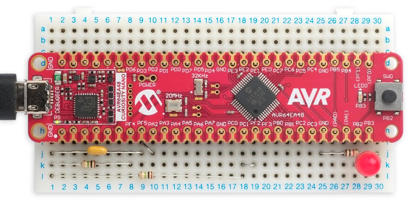
The Blink application using the Event System on an AVR64EA48 Curiosity Nano board.
Push button debouncer
A frequent problem when using push buttons with a microcontroller is that they have contact bounce, which can cause one press on the push button to generate multiple input signals. One approach is to solve the problem in software, by leaving a delay for the contacts to settle before sampling the push button again.
An alternative solution is to add a hardware monostable, to extend the pulse from the push button until after the contacts have settled. Here's a typical circuit:
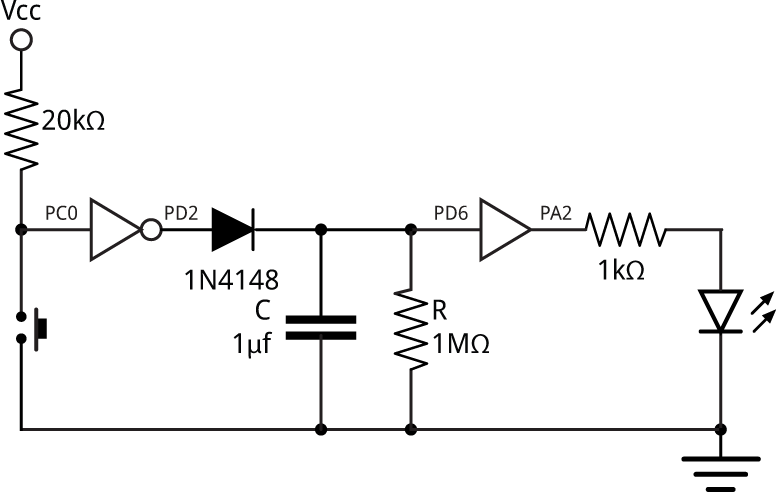
The diode prevents the output PD2 from discharging the capacitor when the push button is released, and it can be any small-signal diode.
The period of this monostable is given by:
T = 0.8 R C = 0.8sec
I chose the 1µF capacitor to give a visible flash so you can see the operation of the circuit, but to debounce a push button a more appropriate value would be about 10 to 15nF, which would give a debounce delay of about 8 to 12msec.
Here's the complete circuit:
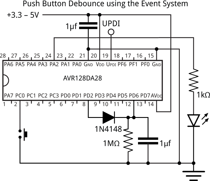
The Event System allows you to implement this without any ICs, and in some cases this will be more convenient than solving it in software.
Here are the settings for the AVR128DA28, or any other Dx series processor:
void setup() {
  // Inverter: Channel 2, PC0 input with pullup, PD2 output
  PORTC.PIN0CTRL = PORT_PULLUPEN_bm;                  // Enable pullup on PC0
  EVSYS.CHANNEL2 = EVSYS_CHANNEL2_PORTC_PIN0_gc;      // PC0 generator on CHANNEL2
  EVSYS.USEREVSYSEVOUTD = EVSYS_USER_CHANNEL2_gc;     // EVOUTD (PD2) CHANNEL2 user
  PORTD.PIN2CTRL = PORT_INVEN_bm;                     // Invert output PD2

  // Buffer: Channel 3, PD6 input, PA2 output
  EVSYS.CHANNEL3 = EVSYS_CHANNEL3_PORTD_PIN6_gc;      // PD6 generator on CHANNEL3
  EVSYS.USEREVSYSEVOUTA = EVSYS_USER_CHANNEL3_gc;     // EVOUTA (PA2) CHANNEL3 user
}

void loop() { }
We avoid the need for the 20kΩ pullup resistor on PC0 by turning on its input pullup.
Here's the circuit connected up on a breadboard:
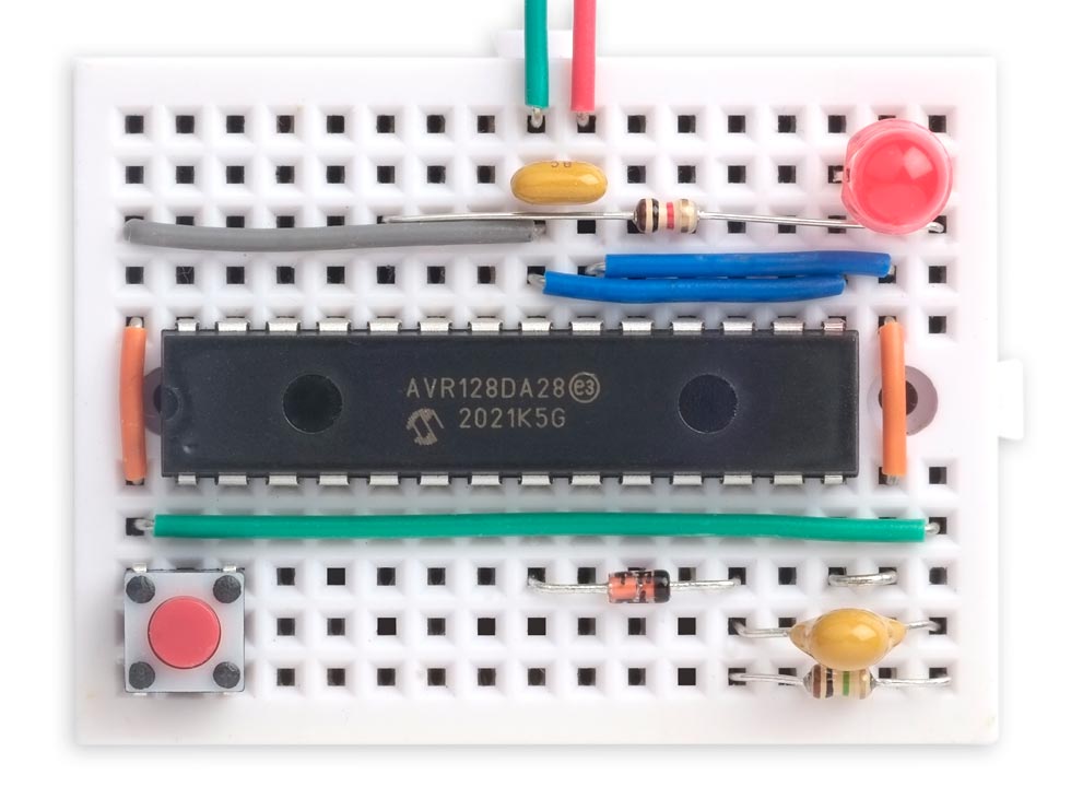
A push button debouncer using the Event System on an AVR128DA28.
Compiling the programs
Compile the programs for the DA, DB, or DD series processors using Spence Konde's Dx Core on GitHub. I tested it with DxCore 1.5.11.
Choose the appropriate option under the DxCore heading on the Board menu; for example AVR DA-series (no bootloader). Check that the Chip option is set as appropriate; for example:
Chip: "AVR128DA28"
You can leave the other options at their defaults.
Then upload each program using a UPDI programmer. The recommended option is to use a USB to Serial board, such as the SparkFun FTDI Basic board [2], connected with a 4.7kΩ resistor as follows:
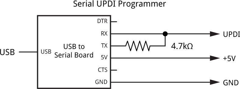
Set the Programmer option to Serial UPDI - 230400 baud. Then choose Upload.
EA and EB series devices
As of DxCore 1.5.11 Serial UPDI doesn't work with the EA or EB series devices [3]. Hopefully this will be fixed in a future release.
To test the Blink example on the AVE64EA48 I therefore used a Curiosity Nano, which allows you to program it by dragging and dropping a .hex file onto a mass storage device. Here's the procedure:
- Compile the program in DxCore by using Export compiled Binary on the Arduino IDE Sketch menu.
- Connect the Curiosity Nano board to your computer's USB port.
A CURIOSITY drive should appear on your desktop.
- Drag the compiled binary .hex file from your program's project folder in the Arduino folder, and drop it onto the CURIOSITY drive.
The PS Power/Status light on the board should flash, and the program will be uploaded to the Curiosity Nano.
- ^ AVR128DA28/32/48/64 Silicon Errata on Microchip.
- ^ SparkFun FTDI Basic Breakout - 5V on SparkFun.
- ^ SerialUPDI does not work with EA-series on GitHub.
blog comments powered by Disqus