Logic Lab
18th May 2023
The Logic Lab provides a selection of 12 logic gates that you can interconnect with patch cables to make a variety of different logic circuits, for experimenting with and learning about logic:

The Logic Lab allows you to experiment with logic gates by interconnecting them with patch cables.
You can enter inputs using switches, and display the outputs on five coloured LEDs. The whole Logic Lab is implemented using a single AVR128DA48 (or ATmega4809) microprocessor and a few LEDs and other passive components, with a total parts cost of under £20 or $25.
I've included nine logic problems that you can try solving with the help of the Logic Lab.
For an alternative version implemented using discrete "1G" CMOS logic gates see Logic Lab 1G.
Introduction
I originally decided to build this for a friend's son who was interested in learning about logic gates, and I thought he would enjoy having something that he could use for practical experiments. I had a design in mind, and searched to see if anything similar already existed; the closest I found was a kit developed by the University of Southampton in the UK [1], but it wasn't commercially available.
My first idea was to use 74LVC series logic gates, which are individual logic gates in small surface-mount packages. The nice thing about this is that each drawing of a logic gate on the PCB would be implemented by a single gate.
However, I then thought about using the Configurable Custom Logic (CCL) in the AVR DA-series microcontrollers, which allows you to configure three-input gates that work independently of the processor. The advantage would be that you could reconfigure the selection of gates in software, without needing to resolder the board. However, even the largest 64-pin devices only provide six logic gates, and in the 48-pin packages it seems that only five of these are actually available on I/O pins.
My final design used an ATmega4809 or AVR128DA48 microcontroller, but simulating the gates by polling the inputs, and setting the outputs accordingly, using truth tables stored in the program. With a 48-pin package it would be possible to emulate at least 12 gates of different types, which would be ample for the design I had in mind. This approach would allow you to change the selection of gates available by uploading a new version of the software, and then making stickers to show the new gate symbols.
Even though the logic gates are simulated using a microcontroller, the only detectable difference is the propagation delay. You can even create an oscillator by connecting the output of one of the inverters back to its input.
Description
The Logic Lab has the following features:
- 12 logic gates: two AND, two NAND, two OR, two NOR, two XOR, and two inverters.
- Four slider switches, S1 to S4, with LEDs to show the status, that can provide logic inputs to the gates.
- Five coloured LEDs, L1 to L5, that can display the state of the output from a logic circuit. The top three are red, orange, and green, allowing simulation of traffic lights.
- Two busses, J1 and J2, that can be used to link patch cables together.
- It is powered by two AAA batteries, with an on/off switch and power indicator LED.
- The inputs and outputs are connected to header pins, so you can interconnect them with a set of patch cables terminated in header sockets.
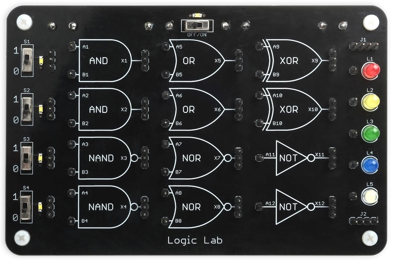
The front panel of the Logic Lab.
Logic problems
Here are nine sample logic problems that you can try solving with the Logic Lab. These can each be solved using the twelve gates in the Logic Lab. I've given an approximate difficulty rating out of 100 for each problem.
For the answers to the problems see Logic Lab Problem Answers.
Traffic lights (15%)
Traffic lights (in the UK) go through the following sequence:
| S1 | S2 | Lights |
| 0 | 0 | Red |
| 0 | 1 | Red and Orange |
| 1 | 0 | Green |
| 1 | 1 | Orange |
Design a logic circuit that lights the red, orange, and green LEDs according to that sequence of switches.
Exclusive-OR (25%)
Two of the gates in the logic lab are exclusive-OR, or XOR, gates; their output is '1' if either of the inputs is '1', but not both.
Design an exclusive-OR gate without using the XOR gates, by using a combination of the other gates in the Logic Lab.
Safety switch (35%)
A school has a fire warning light that lights up in every classroom. To avoid it being accidentally switched on it has four switches, all of which need to be turned on before the warning will light up.
Design a logic circuit that implements this: the red LED, representing the warning, should only turn on if all switches are set to '1'.
Palindrome checker (35%)
Design a circuit that lights the green LED if the four switches are set to a binary number that's a palindrome, such as '1001', and the red LED if it's not a palindrome, like '1011'.
Hotel light switches (40%)
In a hotel four rooms are on the same corridor, and there's one light in the middle of the corridor. There's a switch outside each room that can be used to control the light.
Design a circuit that allows each of the four switches S1 to S4 to turn the light L5 on or off.
Binary decoder (40%)
Design a circuit that lights up just one of the four LEDs L1 to L4 for each of the different possible settings of switches S1 and S2:
| S1 | S2 | Lights |
| 0 | 0 | Red |
| 0 | 1 | Orange |
| 1 | 0 | Green |
| 1 | 1 | Blue |
Majority vote (60%)
When the secret spy club needs to vote on an issue, the three members each have a button that they press to register their vote. If there is a majority vote, the issue is passed.
Use three switches to represent the votes, and design a circuit that will light the green LED if the majority vote '1', or the red LED if they don't.
Combination switch (70%)
You have a drawer with an electronic lock, and it can only be opened if you set the correct password on four switches. Design a logic circuit that allows you to choose any of the 16 possible passwords, such as '1011', by changing the position of four patch leads. The circuit should then only light up the green LED if you set the correct password on the switches.
Binary adder (75%)
Design a circuit that will add together two 2-digit binary numbers, and put the answer in binary on the three LEDs L3 to L5.
The first number should be on S1 (high bit) and S2 (low bit), and the second number should be on S3 (high bit) and S4 (low bit). The answer should be on L3 (high bit), L4 (middle bit), and L5 (low bit).
The circuit
Here's the full circuit of the Logic Lab:
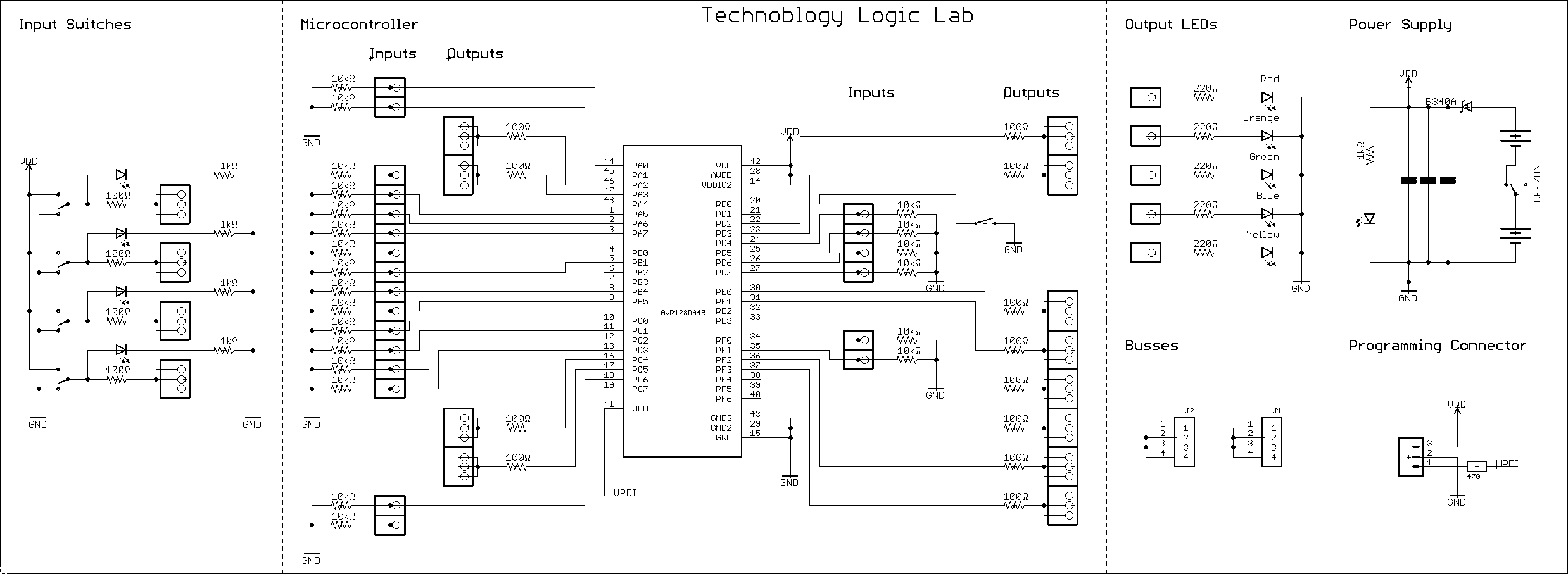
Circuit of the Logic Lab, based on an AVR128DA48 or ATmega4809 processor.
Click to open a larger version in a new window.
There is quite a wide choice of pin-compatible microcontrollers you can use for this project, which should help while many of the most popular parts are still out of stock at time of writing. I built two prototypes, one with an AVR128DA48, and one with the older ATmega4809 which is pin compatible, and their performance was indistinguishable. The program only uses about 1500 bytes, so an ATmega809, ATmega1609, or ATmega3209 should be fine. Likewise, an AVR32DA48 or AVR64DA48 should be fine, or the equivalent AVR32DB parts.
I used 0.1" pitch header pins for the inputs and outputs, and patch leads terminated in header sockets. The advantage of this is that you can buy the header pins in long strips, and then cut them down to the lengths you need; the header sockets are more difficult to divide up.
The five output LEDs are 5mm diffused through-hole LEDs in five different colours. In my first prototype, shown in the photographs, I used a white LED, but found that because white has a higher forward voltage than the other colours, if you connect both white and one of the other LEDs to the same output the white is much dimmer. I therefore replaced white with yellow to avoid the problem.
The other LEDs and resistors are 0805 size SMD types.
The circuit is powered by two 1.5V AAA batteries in series, mounted in through-hole battery clips on the back of the board. Alternatively you could use two PCB-mount AAA battery holders [2] which fit in the same mounting holes.
Short-circuit protection
The board includes 100Ω current limiting resistors on every output, so if the user inadvertently connects together two outputs at different logic levels, the current will be 3/(100 + 100) or 15mA, which is well within the 50mA per output maximum given on the data sheet.
Unconnected inputs
Unconnected inputs are treated as being at logic-level '0'. This is implemented by a 10kΩ pull-down resistor on every input.
If you prefer to have unconnected inputs at logic level '1' (like TTL) you can omit these resistors, and turn on the internal pullup resistors by configuring the inputs as INPUT_PULLUP in setup().
Patch cables
To use the Logic Lab you'll need a set of at least 20 jumper wires terminated in header sockets. I recommend 150mm long cables; either ribbon cables that you can separate to create a set of jumper wires [3], or slightly more expensive separate cables [4].
► Parts list
Construction
I designed a PCB in Eagle and ordered boards from Elecrow [5]. The board is 100 x 140mm, using a double-sided PCB. I also created a design for a back panel and ordered this in 2mm thick transparent acrylic [6]. I give links at the end of the article so you can order your own boards.
The only standard I could find for drawing the logic symbols was a USA Department of Defense document from 1962, which describes how to draw them from arcs of circles [7].
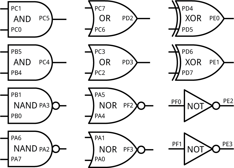
For my first attempt at designing the PCB I assigned the logic gate inputs to the microcontroller ports in a systematic way, with all the AND and NAND gate inputs on one port, all the OR and NOR gate inputs to another port, and so on. However, the layout was a nightmare, and I needed a lot of vias to make it work. I decided to have a second attempt simply choosing the nearest I/O pin to each gate input or output, with the idea that I could sort out in software, and I managed to lay it out much more neatly with no vias.
Here's a guide to the assignment of I/O pins to the gate inputs and outputs:
My recommended sequence for assembling the board is as follows:
- Solder the microcontroller on the back of the board using a hot air gun.
- Solder the SMD resistors and capacitors to the back of the board, and the SMD LEDs to the front of the board, using the hot air gun.
- Fit the the header pins to the front of the board with a conventional soldering iron.
- Mount the switches and 5mm LEDs with a soldering iron.
- Fit the three-pin header socket on the back of the board with a soldering iron.
- Finally, fit the battery holders with a soldering iron, using a generous amount of solder to hold them firmly in place.
For the SMD components I used a Youyue 858D+ hot air gun set to 300°C.
When fitting the header pins I did them a column at a time, and found it helpful to push them into something like a 1x36 header socket [8], to keep them correctly aligned and vertical.
When mounting the battery clips I found I had to enlarge the mounting holes with a 2mm drill to get the clips to fit. You won't need to do this if you use the PCB-mount AAA battery holders [9].
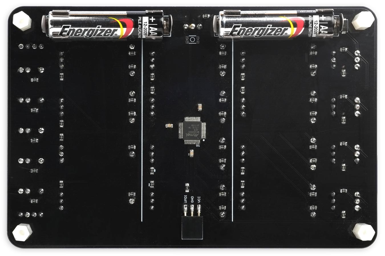
The back of the Logic Lab PCB, showing the ATmega4809 processor and battery holders.
I mounted the transparent acrylic back panel with 15mm nylon pillars [10] and M3 6mm nylon screws [11].
The program
For each gate the program simply reads the inputs, and sets the output according to the truth table for the logic gate.
I thought about using interrupts, but I decided to go with the simpler approach of repeatedly stepping through the gates, processing them in sequence. The program doesn't have anything else to do, so there's no need for interrupts.
Truth tables
The truth table for each of the different gate types is defined by an enum:
enum truthtable_t: uint8_t { AND = 0b1000, NAND = 0b0111,  OR = 0b1110,
                             NOR = 0b0001,  XOR = 0b0110, NOT = 0b0011 };
Logic gate definitions
typedef struct {
  int inputa;
  int inputb;
  int output;
  truthtable_t truthtable;
} gate_t;
This defines the pin numbers used for the two inputs and the output, the value to be output, and the type of logic gate.
Here are the definitions of the 12 gates in the Logic Lab:
gate_t gates[12] = {
  { PIN_PC1, PIN_PC0, PIN_PC5, AND },
  { PIN_PB5, PIN_PB4, PIN_PC4, AND },
  { PIN_PB1, PIN_PB0, PIN_PA3, NAND },
  { PIN_PA6, PIN_PA7, PIN_PA2, NAND },
  { PIN_PC7, PIN_PC6, PIN_PD2, OR },
  { PIN_PC3, PIN_PC2, PIN_PD3, OR },
  { PIN_PA5, PIN_PA4, PIN_PF2, NOR },
  { PIN_PA1, PIN_PA0, PIN_PF3, NOR },
  { PIN_PD4, PIN_PD5, PIN_PE0, XOR },
  { PIN_PD6, PIN_PD7, PIN_PE1, XOR },
  { PIN_PF0, PIN_PF0, PIN_PE2, NOT },
  { PIN_PF1, PIN_PF1, PIN_PE3, NOT },
};
For simplicity I define the NOT gate as a two input gate where both inputs are the same pin.
If you wanted to change the type of a gate simply change its truthtable value in this table. For example, you could change all the two-input gates into NAND gates by changing their definitions to NAND, or you could add some XNOR gates by also defining them in truthtable_t.
Configuring the outputs
In setup() the appropriate I/O pins are configured as outputs:
void setup () {
  // Set outputs
  for (int i=0; i<12; i++) {
    pinMode(gates[i].output, OUTPUT);
  }
}
Processing the gates
Finally in loop() we repeatedly scan through each gate, read the inputs, and set the output according to the gate's truth table:
void loop () {
  for (int i=0; i<12; i++) {
    gate_t gate = gates[i];
    bool ina = digitalRead(gate.inputa);
    bool inb = digitalRead(gate.inputb);
    int val = ina << 1 | inb;
    bool out = (gate.truthtable >> val) & 1;
    digitalWrite(gate.output, out);
  }
}
That's all there is to it.
Compiling the program
AVR128DA48
If you're using an AVR128DA48, or anything from the AVR32DA48 or AVR32DB48 upwards, compile the program using Spence Konde's Dx Core on GitHub (I used 1.5.3). Choose the AVR DA-series (no bootloader) or AVR DB-series (no bootloader) option as appropriate under the DxCore heading on the Board menu. Check that the subsequent options are set as follows (ignore any other options):
Chip: "AVR128DA48" or "AVR128DB48"
Clock Speed: "4 MHz internal"
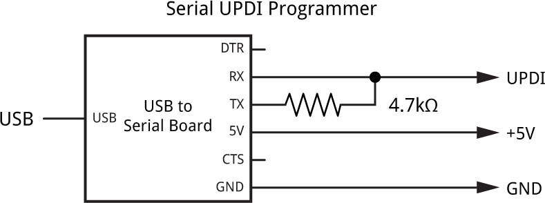
Then upload the program to the processor on the breadboard using a UPDI programmer connected to the GND, +5V, and UPDI pins.
The recommended option is to use a USB to Serial board, such as the SparkFun FTDI Basic board [12], or a USB to Serial cable [13], connected with a 4.7kΩ resistor as follows:
- Set Programmer to the first of the "SerialUPDI - 230400 baud" options.
- Select the USB port corresponding to the USB to Serial board in the Port menu.
- Choose Upload from the Arduino IDE Tools menu to upload the program.
Using a clock speed of 4MHz reduces the processor power consumption from 4.7mA to 1.1mA.
ATmega4809
If you're using an ATmega4809, or anything from the ATmega809 upwards, compile the program using MCUdude's MegaCoreX on GitHub. Choose the ATmega4809 option as appropriate under the MegaCoreX heading on the Board menu. Check that the subsequent options are set as follows (ignore any other options):
Clock: "Internal 4 MHz"
BOD: "BOD disabled"
Pinout: "48 pin standard"
On the ATmega4809, choosing a clock speed of 4MHz ensures that the processor will run down to the minimum voltage of 1.8V, for maximum battery life.
Then upload the program using a USB to Serial board, as described above. See the MegaCoreX documentation for further details.
Resources
Here's the Logic Lab program: Logic Lab Program.
Get the Eagle files or Gerber files for the PCB on GitHub here: https://github.com/technoblogy/logic-lab.
Or order boards from OSH Park here: Logic Lab.
Acknowledgements
Thanks to Dashi for encouraging me to build this, and to Chris Jordan for collaborating on the design.
- ^ A-Level Computer Science Logic and Arithmetic Kit on the University of Southampton website.
- ^ AAA x 1 Battery Holder PCB Mount on Switch Electronics.
- ^ Premium Female/Female Jumper Wires on The Pi Hut.
- ^ Jumper Wires 10pk (Female/Female) on The Pi Hut.
- ^ PCB Fab on Elecrow.
- ^ Acrylic Laser Cutting on Elecrow.
- ^ MIL-STD-806B Graphical Symbols for Logic Diagrams on bitsavers.org.
- ^ 36-pin 0.1" Female header on The Pi Hut.
- ^ AAA x 1 Battery Holder PCB Mount on Switch Electronics.
- ^ 15mm nylon pillars on Switch Electronics.
- ^ M3 x 6mm nylon screws on Switch Electronics.
- ^ SparkFun FTDI Basic Breakout - 5V on Sparkfun.
- ^ FTDI Serial TTL-232 USB Cable on Adafruit.
blog comments powered by Disqus