Combination Lock Using CCL
30th November 2020
This project is a digital combination lock that only lets you activate a circuit if you know the 8-bit key. It demonstrates an application of Configurable Custom Logic, a feature included in the latest AVR DA-series chips from Microchip:
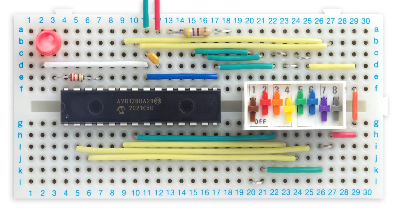
Combination Lock implemented using Configurable Custom Logic on an AVR128DA28.
The key is 10010011.
As a comparison, I implement the same application using a conventional program, and discuss the pros and cons of each approach.
Introduction
The latest AVR processors released by Microchip all include a new feature called Configurable Custom Logic, or CCL, and since their release I've been trying to think of compelling applications of this feature. It allows you to construct an arbitrary logic circuit that works independently of the processor. This project demonstrates one practical application, using the logic functions to construct an arbitrary logic expression.
CCL is included in three ranges of AVR devices: the new ATtiny 0-series and 1-series, the new ATmega 0-series, and the AVR DA series which Microchip announced in May of this year. I decided to use one of the AVR DA series; although most of the parts are in surface-mount packages, they have fortunately made the AVR128DA28 available in a 28-pin DIP package which is ideal for experimenting with on a prototyping board. Spence Konde already has an Arduino core called DxCore available for the DA series [1], and this includes instructions for making yourself a suitable UPDI programmer.
By the way, if like me you're familiar with the way in which the old ATtiny and ATmega processor registers are configured, you may find the naming conventions used in the DA series quite confusing. I recommend reading Microchip's document Getting Started Writing C-code for XMEGA, which explains the conventions, and the rationale behind them; thanks to @awneil on AVR Freaks for suggesting this.
CCL logic elements
To understand how to configure the CCL I found I needed to spend some time reading the appropriate chapter in the datasheet [2]. Essentially the CCL provides configurable logic elements, sequencing blocks such as flip-flops and latches, and signal conditioning such as filters and edge-detectors. In this project I am just using the logic elements.
Each configurable logic element has three inputs and one output, and you can construct more complex circuits by combining these. The AVR DA series devices provide four logic elements on the 28-pin and 32-pin parts, and six logic elements on the 48-pin and 64-pin parts. The following table shows the pins corresponding to each of the four logic elements available on the smaller packages, and the pin numbers in brackets show the I/O pins available on the 28-pin parts:
| IN0 | IN1 | IN2 | OUT | |
| LUT0 | PA0 (22) | PA1 (23) | PA2 (24) | PA3 (25) |
| LUT1 | PC0 (2) | PC1 (3) | PC2 (4) | PC3 (5) |
| LUT2 | PD0 (6) | PD1 (7) | PD2 (8) | PD3 (9) |
| LUT3 | PF0 (16) | PF1 (17) | PF2 | PF3 |
Fortunately the 28-pin parts have enough inputs assigned to pins to allow you to cascade four of the logic elements and make an 8-input general logic gate:
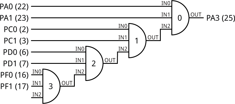
Arrangement of CCL logic elements to implement the Combination Lock.
The Combination Lock uses this configuration to allow you to set an 8-bit input, using a DIP switch, and only if you set the correct combination will the output go high and light the LED.
The circuit
Here's the circuit of the Combination Lock, using a similar layout to the circuit on the prototyping board:
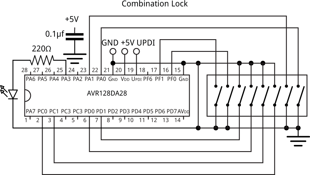
Circuit of the Combination Lock using an AV128DA28.
The processor is an AVR128DA28 in an SPDIP package [3], and the DIP switch is an 8-way single-throw type [4].
Combination Lock using CCL
Here's the CCL version of the Combination Lock. This is all done in setup().
Configuring the inputs
First we define the eight inputs with pullups, so when not switched to GND by the DIP switch they read as logic high:
  PORTA.PIN0CTRL = PORT_PULLUPEN_bm;                     // Pullup on PA0
  PORTA.PIN1CTRL = PORT_PULLUPEN_bm;                     // Pullup on PA1
  PORTC.PIN0CTRL = PORT_PULLUPEN_bm;                     // Pullup on PC0
  PORTC.PIN1CTRL = PORT_PULLUPEN_bm;                     // Pullup on PC1
  PORTD.PIN0CTRL = PORT_PULLUPEN_bm;                     // Pullup on PD0
  PORTD.PIN1CTRL = PORT_PULLUPEN_bm;                     // Pullup on PD1
  PORTF.PIN0CTRL = PORT_PULLUPEN_bm;                     // Pullup on PF0
  PORTF.PIN1CTRL = PORT_PULLUPEN_bm;                     // Pullup on PF1
Configuring the Look-Up Tables
Next we configure the four LUTs to take IN0 and IN1 from external pins, and IN2 from a link to the output of the next LUT in all cases except LUT3:
  CCL.LUT0CTRLB = CCL_INSEL0_IN0_gc | CCL_INSEL1_IN1_gc; // Inputs 0 and 1 from pins
  CCL.LUT0CTRLC = CCL_INSEL2_LINK_gc;                    // Input 2 from next LUT
  CCL.LUT1CTRLB = CCL_INSEL0_IN0_gc | CCL_INSEL1_IN1_gc; // Inputs 0 and 1 from pins
  CCL.LUT1CTRLC = CCL_INSEL2_LINK_gc;                    // Input 2 from next LUT
  CCL.LUT2CTRLB = CCL_INSEL0_IN0_gc | CCL_INSEL1_IN1_gc; // Inputs 0 and 1 from pins
  CCL.LUT2CTRLC = CCL_INSEL2_LINK_gc;                    // Input 2 from next LUT
  CCL.LUT3CTRLB = CCL_INSEL0_IN0_gc | CCL_INSEL1_IN1_gc; // Inputs 0 and 1 from pins
  CCL.LUT3CTRLC = CCL_INSEL2_MASK_gc;                    // Input 2 masked
Defining the truth tables
For each LUT we need to define a truth table, specifying what state the output should be for the eight possible states of the inputs. The truth table is specified by an 8-bit number; each bit specifies the output for one set of states of the inputs. So, for example, bit 6 in the truth table specifies the state of the output for IN2 = 1, IN1 = 1, and IN0 = 0.
For our combination lock we only want the output to be '1' if the inputs IN2, IN1, and IN0 are in the correct states, so the truth table is an eight-bit binary number with one '1' bit. An easy way to calculate it is:
1 << 0bxxx
where xxx is the binary number representing the inputs on IN2, IN1, and IN0 respectively.
As an example we'll define the Key as:
const int Key = 0b10010011;
So the truth table for LUT3 is:
1 << 0b010
because IN2 is ignored (so zero), and IN1 and IN0 are the top two bits of the Key, '10'.
The truth table for LUT2 is:
1 << 0b101
because IN2 must be '1' from the previous LUT, and IN1 and IN0 are the next two bits of the Key, '01'. LUT1 and LUT0 are calculated in the same way.
We can define the truth tables to cater for any specified key as follows:
  CCL.TRUTH0 = 1<<(0b100 | (Key & 0b11));                // Truth table for LUT0
  CCL.TRUTH1 = 1<<(0b100 | (Key>>2 & 0b11));             // Truth table for LUT1
  CCL.TRUTH2 = 1<<(0b100 | (Key>>4 & 0b11));             // Truth table for LUT2
  CCL.TRUTH3 = 1<<(0b000 | (Key>>6 & 0b11));             // Truth table for LUT3
For the particular key given above these are equivalent to:
  CCL.TRUTH0 = 1 << 0b111;
  CCL.TRUTH1 = 1 << 0b100;
  CCL.TRUTH2 = 1 << 0b101;
  CCL.TRUTH3 = 1 << 0b010;
Enabling the LUTs and CCL
Then finally we enable the LUTs, and the whole CCL:
  CCL.LUT0CTRLA = CCL_ENABLE_bm | CCL_OUTEN_bm;          // LUT0 and output to pin
  CCL.LUT1CTRLA = CCL_ENABLE_bm;                         // LUT1
  CCL.LUT2CTRLA = CCL_ENABLE_bm;                         // LUT2
  CCL.LUT3CTRLA = CCL_ENABLE_bm;                         // LUT3
  CCL.CTRLA = CCL_ENABLE_bm | CCL_RUNSTDBY_bm;           // CCL, run in standby
For LUT0 we also specify that its output is sent to a pin. Note that there's no need to also define the pin as an output; this happens automatically.
This final step must be performed last, because the LUT control registers are protected from being configured while the LUTs are enabled.
Once the CCL is enabled, the logic elements perform their task irrespective of what the program is doing.
Here's the whole Combination Lock CCL version: Combination Lock CCL.
Combination Lock using a program
Now, for comparison, here's how I would implement the same application using a program.
First, here's the key:
const int Key = 0b10010011;
Next, as before, we define pullups on the eight inputs, and define PA3 as an output:
void setup() {
  // Configure I/O pins appropriately
  PORTA.PIN0CTRL = PORT_PULLUPEN_bm;                     // Pullup on PA0
  PORTA.PIN1CTRL = PORT_PULLUPEN_bm;                     // Pullup on PA1
  PORTC.PIN0CTRL = PORT_PULLUPEN_bm;                     // Pullup on PC0
  PORTC.PIN1CTRL = PORT_PULLUPEN_bm;                     // Pullup on PC1
  PORTD.PIN0CTRL = PORT_PULLUPEN_bm;                     // Pullup on PD0
  PORTD.PIN1CTRL = PORT_PULLUPEN_bm;                     // Pullup on PD1
  PORTF.PIN0CTRL = PORT_PULLUPEN_bm;                     // Pullup on PF0
  PORTF.PIN1CTRL = PORT_PULLUPEN_bm;                     // Pullup on PF1
  PORTA.DIR = PIN3_bm;                                   // Pin PA3 as output
}
Then, in loop(), we read the settings of the I/O lines corresponding to the DIP switch, and if they match Key light the LED:
void loop() {
 int bits10 = PORTA.IN & (PIN1_bm | PIN0_bm);
 int bits32 = PORTC.IN & (PIN1_bm | PIN0_bm);
 int bits54 = PORTD.IN & (PIN1_bm | PIN0_bm);
 int bits76 = PORTF.IN & (PIN1_bm | PIN0_bm);
 int combination = bits76<<6 | bits54<<4 | bits32<<2 | bits10;
 if (combination == Key) PORTA.OUT |= PIN3_bm;          // Write PA3 high
 else PORTA.OUT &= ~PIN3_bm;                            // Write PA3 low
 delay(1000);
}
I could have made it a bit simpler by connecting the DIP switch to eight I/O lines in the same port, such as PD0 to PD7 in the AVR128DA28, but I wanted to use the same prototyping board layout.
Here's the whole Combination Lock program version: Combination Lock Program.
Compiling the programs
Compile the programs using Spence Konde's Dx Core on GitHub. Choose the AVR DA-series (no bootloader) option under the DxCore heading on the Board menu. Check that the subsequent options are set as follows (ignore any other options):
Chip: "AVR128DA28"
Clock Speed: "24 MHz internal"
Programmer: "jtag2updi (megaTinyCore)"
Then upload the program to the processor on the breadboard using a UPDI programmer connected to the GND, +5V, and UPDI pins. You can make a UPDI programmer from an Arduino Uno, or other ATmega328P-based board, as described in Make UPDI Programmer.
The programs should also work perfectly well on any other AVR DA-series devices, and at other clock speeds.
Conclusion
Obviously this Combination Lock is more of a demonstration than a practical security device, as it wouldn't take long to test all 256 combinations. However, it could be made more secure in conjunction with a button to submit a test combination, together with an increasing time delay penalty for incorrect attempts. Alternatively, using all six LUTs in the larger AVR DA devices you could create a combination lock with a key of up to 13 bits.
Pros and cons of each approach
Using the Configurable Custom Logic is a lot more work to set up, but once configured it provides the application without any load on the processor, which could be performing a highly intensive task, such as outputting a digital waveform, without any interruption from the operation of the combination lock.
Another advantage of the CCL approach is that it continues to work when the processor is asleep. I measured the current consumption with the LED not lit: for the program version it was 6.9mA, whereas for the CCL version in power-down sleep mode it was only 1.3mA.
There are however some limitations of the CCL approach. Because the logic circuit must be constructed from three-input components some logic circuits can't be implemented. One example would be a combination lock that is only activated by an 8-bit number with the same number of '0's and '1's, such as 0b10110001. Implementing this using the program version would be a relatively simple extension.
In conclusion, CCL is probably going to be most useful in applications that would normally need a few additional logic gates, but which can now be implemented entirely with a single microcontroller chip.
Update
1st December 2020: Corrected the information about the number of LUTs on the different DA-series parts.
- ^ DxCore on GitHub.
- ^ AVR128DA28/32/48/64 datasheet on Microchip.
- ^ AVR128DA28-I/SP on Mouser.co.uk.
- ^ 8 Way Through Hole DIP Switch on RS-Online.
blog comments powered by Disqus