Using a Timer on the Arduino Uno or Arduino Zero
29th December 2021
This article compares how you can configure a timer to blink an LED, or generate a waveform, on the ATmega328P microcontroller on the Arduino Uno, and the ATSAMD21 microcontroller on the Arduino Zero:
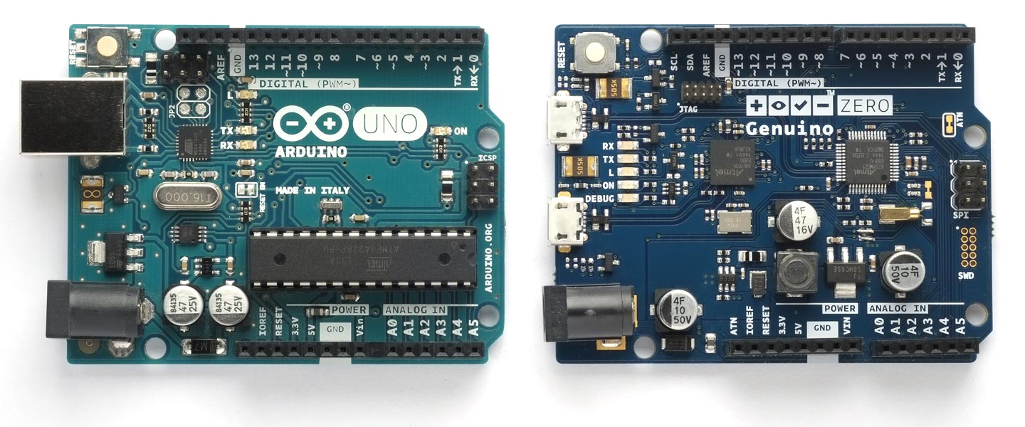
The Arduino Uno, based on the AVR ATmega328P, and the Arduino Zero,
based on the ARM ATSAMD21.
I thought it would be an interesting exercise to compare how you approach the same task on AVR and ARM processors, and the programs will work on most other boards based on the same processors.
Introduction
Most microcontrollers include one or more timer peripherals that allow you to time precise intervals and generate waveforms on output pins. In this example I'm going to use a timer to toggle an LED connected to an I/O pin. Like the original Arduino Blink example the LED will be flashed at exactly 0.5Hz; one second on and one second off.
There are two ways to do this:
- One way is to use the timer to generate a regular interrupt, and then toggle the I/O line in the interrupt service routine.
- The other way, which is the way I'll use, is to configure the timer to directly toggle an output pin.
The advantage of the second approach is that it's simpler, and the output waveform will be precise, with no jitter due to the time taken to respond to the interrupt. Also, because there's no overhead from executing the interrupt it's capable of generating higher frequencies, typically up to about half the clock frequency. This is a good way of quickly setting up a source of a square wave with a precise frequency.
Figuring out how to program peripherals directly, rather than using the Arduino functions, typically involves a lot of digging into the appropriate microcontroller datasheet. In the following descriptions I include links to the appropriate page in each datasheet. Note that these page links work on most browsers, but unfortunately not on Safari. If you're using Safari the link will just open the datasheet at the first page, and you'll have to scroll to the correct page in the datasheet manually; alternatively, copy and paste the URL into the address bar of another browser.
AVR
For the AVR version of the Blink example I'll use the ATmega328P on the Arduino Uno.
The ATmega328P has three Timer/Counter peripherals. Timer/Counter0 is used for millis() and Timer/Counter2 is used for tone(), so this example uses the 16-bit Timer/Counter1.
Timer/Counter1 is hardwired to generate waveforms on the following two I/O lines:
- OC1A - PB1 (Arduino Pin 9)
- OC1B - PB2 (Arduino Pin 10)
In these examples we have to deal with the fact that the microcontroller uses one system of numbering I/O pins, grouping the pins into ports, but the Arduino board numbers the pins using consecutive integers.
For this example we'll use Arduino pin 10, which is bit 2 in port B. For this example you'll need to connect an LED in series with a 220Ω resistor between pin 10 and GND:
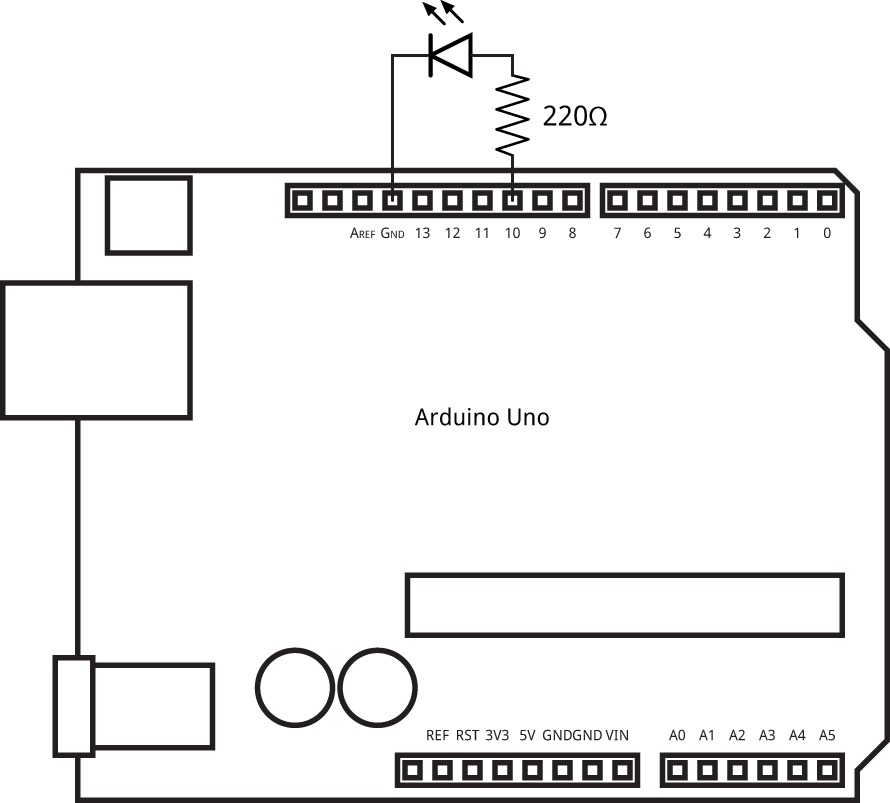
Connecting an LED to the Arduino Uno or Arduino Zero to be blinked by a timer.
Defining the port registers
The first step is to use the Data Direction Register to define this pin as an output. The I/O port registers are defined in Section 14.4, page 100, in the ATmega328P Datasheet:
DDRB = DDRB | 1<<DDB2; // Make PB2 an output
Defining the timer registers
The timer/counter's registers are described in Section 16.11, page 140, in the ATmega328P Datasheet. The timer mode we want is CTC (Clear Timer on Compare), which counts up to the 16-bit value in register OCR1A. This mode is specified by the bits WGM13 to WGM10 set to '0100'. The bottom two bits are in register TCCR1A and the top two in register TCCR1B.
We also want to set the bits COM1B1 and COM1B0 to '01' to toggle the output pin OC1B every cycle, and the bits CS12 to CS10 to '101' to prescale the clock by 1024:
  TCCR1A = 0b01<<COM1B0 | 0b00<<WGM10;   // Toggle OC1B on match, CTC mode
  TCCR1B = 0b01<<WGM12 | 0b101<<CS10;    // CTC mode, divide by 1024
Finally we need to specify the value in the output compare register, OCR1A, to get the correct output frequency. To do this we need to put the value 15624 into register OCR1A; it's one less than the divisor we want because the counter counts from zero.
OCR1A = 15624; // Divide by 15625
The clock frequency is 16MHz, so the output will be toggled at a frequency of 16000000/1024/(15624+1) or 1Hz. Because the output is toggling, this is a square wave with a frequency of 0.5Hz.
The whole program for the ATmega328P
Here's the whole program. It's just 4 lines of C:
void setup() {
  DDRB = DDRB | 1<<DDB2;                 // Make PB2 an output
  TCCR1A = 0b01<<COM1B0 | 0b00<<WGM10;   // Toggle OC1B on match, CTC mode
  TCCR1B = 0b01<<WGM12 | 0b101<<CS10;    // CTC mode, divide by 1024
  OCR1A = 15624;                         // Divide by 15625
}
When you upload this the LED will blink at 0.5Hz.
ARM
Programming the ARM peripherals is generally more complicated than for the earlier AVR processors because of three considerations:
- Some registers are enable-protected, and can only be written when the peripheral is disabled.
- After writing to some registers the change must be synchronized by waiting for a synchronization flag before proceeding.
- After writing to some registers you need to wait until the operation has completed before proceeding.
These are explained in greater detail as I work through the example.
For the ARM version of the Blink example I'll use the ATSAMD21G18A used on the Arduino Zero. This has three TC Timer/Counters and three TCC Timer/Counters. I'll use TC3, because the waveform outputs, referred to as TC3[0] and TC3[1], are on convenient pins on the board.
On the ARM processors signals can generally be routed to several alternative I/O pins using the PORT I/O Pin Controller. For details see Section 7.1, page 29, in the ATSAMD21 Datasheet. For example, the TC3 waveform outputs have these two alternatives:
| Waveform output | ||
| TC3[0] | PA14 (2) | PA18 (10) |
| TC3[1] | PA15 (5) | PA19 (12) |
The numbers in brackets are the Arduino pin numbers on the Arduino Zero.
For this example I'll use TC3[0] on pin PA18, which is Arduino pin 10 on the Arduino Zero (coincidentally the same pin as we used for the Arduino Uno example).
This example will work on any ATSAMD21-based board, but note that the Arduino pin numbers may be different. Check the schematic for the board you're using to check which pin corresponds to PA18. Here's a table showing which Arduino pin you need to connect the LED to on some other popular boards:
| Board | PA18 pin |
| Arduino Zero | D10 |
| Adafruit Feather M0 | D10 |
| Adafruit ItsyBitsy M0 | D10 |
| Adafruit Metro M0 | D10 |
| Seeduino XIAO | Rx LED * |
| Adafruit QT-Py | n/a |
| Adafruit Gemma M0 | n/a |
| Arduino MKRZero | n/a |
* The Seeduino XIAO has the blue Rx LED connected to PA18, so you don't need to connect an LED.
The boards marked n/a don't make PA18 available on an output pin and so can't be used with this program as it stands.
Selecting the clock for TC3
The first step is to select the clock to use as the source for TC3. In this case we will use the 48MHz system clock, GCLK0.
To do this we use the Generic Clock Controller peripheral, GCLK. Specifically we need to program the CLKCTRL register. For details see Section 15.8.3, page 122, in the ATSAMD21 Datasheet.
The command is:
  GCLK->CLKCTRL.reg = GCLK_CLKCTRL_CLKEN |
    GCLK_CLKCTRL_GEN_GCLK0 | GCLK_CLKCTRL_ID_TCC2_TC3;      // Use GCLK0 for TC3
The meaning of this is as follows:
- GCLK->CLKCTRL.reg refers to the Generic Clock Control register.
- GCLK_CLKCTRL_CLKEN enables the clock.
- GCLK_CLKCTRL_GEN_GCLK0 specifies GCLK0, the 48MHz system clock.
- GCLK_CLKCTRL_ID_TCC2_TC3 assigns it to TC3 (and TCC2).
Resetting Timer/Counter TC3
The next step is to reset Timer/Counter TC3 by setting the SWRST bit in the register CTRLA in TC3. Although not strictly necessary, it ensures that no previous configuration of TC3 interferes with our application. For details see Section 30.8.1, page 571, in the ATSAMD21 Datasheet.
  TC3->COUNT16.CTRLA.reg = TC_CTRLA_SWRST;                  // Reset TC3
  while (TC3->COUNT16.CTRLA.bit.SWRST);                     // Wait for completion
The while statement waits until the reset has completed. When the timer has been reset it is disabled.
Assigning the port pin to TC3
To make pin PA18 work with the timer/counter you need to assign it to the TC peripheral in the PORT peripheral WRCONFIG register. For details see Section 23.8.11, page 383, in the ATSAMD21 Datasheet. The command is:
PORT->Group[0].PINCFG[18].bit.PMUXEN = PORT_PINCFG_PMUXEN;// Enable PMUX for PA18
The meaning of this is as follows:
- PORT->Group[0] refers to PORT A. PORT B would be PORT->Group[1].
- PINCFG[18] means we want to configure pin 18 in that port; ie PA18.
- PORT_PINCFG_PMUXEN enables the Peripheral Multiplexer for this pin.
Next we need to assign the pin to the TC peripheral in the PORT peripheral PMUX register. For details see Section 23.8.12, page 385, in the ATSAMD21 Datasheet. The command is:
PORT->Group[0].PMUX[9].bit.PMUXE = PORT_PMUX_PMUXE_E; // Assign PA18 to TC3
The meaning of this is as follows:
- PORT->Group[0] refers to PORT A, as before.
- PMUX[9] means we want to configure the 9th pair of pins; ie PA18 and PA19.
- PMUXE means we want to configure the even-numbered pin of the pair; ie PA18.
- PORT_PMUX_PMUXE_E means we want to assign it to column E in the table in Section 7.1, page 29, in the ATSAMD21 Datasheet.
Note that we don't need to define PA18 as an output; this is implied by setting it as a waveform output for TC3.
Enabling the clock for TC3
The next step is to use the Power Manager peripheral to enable the clock to TC3. The TC3 peripheral is clocked by the APBC clock, and to enable it we need to set the appropriate bit in the APBCMASK register. For details see Section 16.8.10, page 151, in the ATSAMD21 Datasheet.
PM->APBCMASK.reg = PM->APBCMASK.reg | PM_APBCMASK_TC3; // Enable clock for TC3
Configuring TC3
Now we need to configure TC3 using the register CTRLA in TC3 again. For details see Section 30.8.1, page 571, in the ATSAMD21 Datasheet.
  TC3->COUNT16.CTRLA.reg = TC_CTRLA_MODE_COUNT16 |          // 16-bit mode
    TC_CTRLA_WAVEGEN_MFRQ | TC_CTRLA_PRESCALER_DIV1024;     // MFRQ mode, / 1024
The meaning of this is as follows:
- TC_CTRLA_MODE_COUNT16 sets the timer/counter into 16-bit mode.
- TC_CTRLA_WAVEGEN_MFRQ selects Match Frequency mode, which uses the register CC0 to determine the frequency.
- TC_CTRLA_PRESCALER_DIV1024 selects a prescaler of 1024, to divide the clock by 1024.
Setting the divisor
The output frequency will be determined by the divisor programmed into the TC3 register CC0. For details see Section 30.12.13, page 615, in the ATSAMD21 Datasheet.
  TC3->COUNT16.CC[0].reg = 46874;                           // Divide clock by 46875
  while (TC3->COUNT16.STATUS.reg & TC_STATUS_SYNCBUSY);     // Synchronize
The clock frequency is 48MHz, so the output will be toggled at a frequency of 48000000/1024/(46874+1) or 1Hz. Because the output is toggling, this is a square wave with a frequency of 0.5Hz.
This register is write-synchronized, so we need to wait until the SYNCBUSY bit in the STATUS register is zero before proceeding.
Enabling the timer/counter
The final step is to enable the counter, to start it counting, by setting the ENABLE bit in CTRLA:
  TC3->COUNT16.CTRLA.reg |= TC_CTRLA_ENABLE;                // Enable TC3
  while (TC3->COUNT16.STATUS.reg & TC_STATUS_SYNCBUSY);     // Synchronize
This bit is write-synchronized, so as before we need to wait until the SYNCBUSY bit in the STATUS register is zero before proceeding.
The whole program for the ATSAMD21
Here's the whole program:
void setup() {
  GCLK->CLKCTRL.reg = GCLK_CLKCTRL_CLKEN |
    GCLK_CLKCTRL_GEN_GCLK0 | GCLK_CLKCTRL_ID_TCC2_TC3;      // Use GCLK0 for TC3

  TC3->COUNT16.CTRLA.reg = TC_CTRLA_SWRST;                  // Reset TC3
  while (TC3->COUNT16.CTRLA.bit.SWRST);                     // Wait for completion

  PORT->Group[0].PINCFG[18].bit.PMUXEN = PORT_PINCFG_PMUXEN;// Enable PMUX for PA18
  PORT->Group[0].PMUX[9].bit.PMUXE = PORT_PMUX_PMUXE_E;     // Assign PA18 to TC3
  PM->APBCMASK.reg = PM->APBCMASK.reg | PM_APBCMASK_TC3;    // Enable clock for TC3
  TC3->COUNT16.CTRLA.reg = TC_CTRLA_MODE_COUNT16 |          // 16-bit mode
    TC_CTRLA_WAVEGEN_MFRQ | TC_CTRLA_PRESCALER_DIV1024;     // MFRQ mode, / 1024

  TC3->COUNT16.CC[0].reg = 46874;                           // Divide clock by 46875
  while (TC3->COUNT16.STATUS.reg & TC_STATUS_SYNCBUSY);     // Synchronize

  TC3->COUNT16.CTRLA.reg |= TC_CTRLA_ENABLE;                // Enable TC3
  while (TC3->COUNT16.STATUS.reg & TC_STATUS_SYNCBUSY);     // Synchronize
}
When you upload this the LED will blink at 0.5Hz.
blog comments powered by Disqus